![]()
AC current sensor·Application circuit 1
1.Current input AC amplified circuit
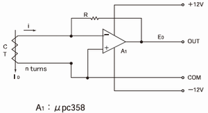
· It is for micro current measurement to be 0V on the output voltage of CT equivalently.
(Suitable for i=I0/n<5mA)
· Output voltage E0= i·R(Vrms)
· The OP amp should be selected as low offset and low noise type in the cause of micro signal level.
2.Voltage input AC amplified circuit
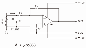
· It amplify the voltage, after the output current of CT is
converted to the voltage e0 with RL.
(Suitable for i=I0/n>5mA)
· CT output voltage e0=K·I0·RL/n(Vrms)
· Output voltage E0=e0·R2/R1(Vrms)
· To use CT with maximum characterization, RL value should be lower.
Even if the e0 value is small, the signal can be amplified.
· R3 is the parallel resistance of R1 and R2.
3.Average value of rectification type current converting circuit
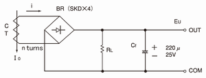
· Output voltage E0=0.9·K·I0·RL/n(VDC)
(0.9:Vrms→VDC converting constant)
· RL should be connected at the DC side to cancel the drop of the forward voltage on the diode.
· It is hopeful to use the schottky diode with low drop of the forward voltage.
· The Cf value is decided by the good balance of the response time and the acceptable ripple voltage.
4.Single power supply DC output amplified circuit
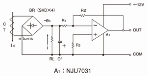
· CT output voltage (as 0.1-1V around)
-e0=0.9·K·I0·RL/n(VDC)
· Output E0=e0·R2/R1(VDC)
· R3 is the parallel resistor of R1 and R2.
· Because the amplifier act as the inverting amplifier for the minus input, the output can be gotten by the single power supply. However, the amplifier of low saturation type should be selected to act from around 0V.
5.Bi-polar power supply DC output amplified circuit
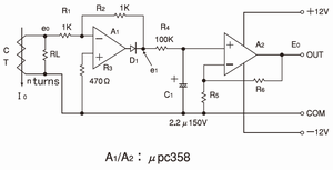
· The first stage amplifier (as 0.1-1V output)
It is the ideal rectifier circuit with R1, R2, A1, D1.
e0=K·I0·RL/n(Vrms)
e1=0.9·e0 (VDC)
· R4 and C1 are low pass filter.
· A2, R5, and R6 are buffer amplifier
E0=e1·(R5+R6)/R5(VDC)
· It can gain absolute value output with acting from 0V/0A.
6.High precision over load detection circuit (single power supply)
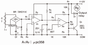
· It is same as 4. of circuit example until A1 output.
· It can adjust the ON level with ZD1 and trimmer for setting.
· A2 is the comparator circuit with the OP amp for the protection toward jitter by hysteresis function.
· The calculation of hysteresis range VTH is
VTH=R5(VH-VL)/(R5+R6)
VH≈12V·R8 /(R7+R8)
VL≈0V
7.Instantaneous operating type over load detection (single power supply)
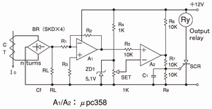
· It is same as 4. of circuit example until A1 output.
However, Cf is deleted for the instantaneous behavior.
· A2 is the high precision comparator with the op-amp.
· It can set up the output latch of acting with SCR.
It can protect with C1 about the malfunction of SCR's gate and set up the delay of the operation, slightly.
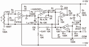
8.4-20mA current converting circuit (for single power supply)
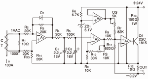
·The example of (0-100Arms)→(4-20mADC) converting
· A1:CT output rectifier circuit
· A2:Buffer amplifier for 4mA offset
It is trimmer set up of (OS) for4mA output at 0A.
· A3:Buffer amplifier for 20mA full scale
It is trimmer set up of (FS) for 20mA output at 100A.
· A4:Same phase adding amplifier to compare between
A2, A3 output, and feedback signal from R12.
9.4-20mA current converting circuit (for bi-polar power supply)
· A1:Absolute value rectifier circuit for CT's output (-output)
· A2:Buffer amplifier for DC value of CT's output
· A3:Adding amplifier for 4-20mA output
4mA trimmer set up (OS) at 0A
20mA trimmer set up (FS) at 100A
· A4:Differential amplifier for feedback of output current
· Although it is operated with ±12V power supply, the terminator of load side is limited below 400Ω.
10.CT sensitivity programmable type
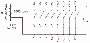
· The right picture is the example of the structure to be able to set up the load resistor to get 1V output as 1A step from 1A-100A with CTU-8-S50-60.
The sum of the current value at the ON position is setted sensitivity. (ex:1A+4A+20A+30A=55A)
· The point to select CT
It should be structured with CT of flat characteristic of (K) value during the applied current range, and the lowest resistor value as possible.
![]()
![]()
![]()
![]()
![]()